- 您现在的位置:买卖IC网 > Sheet目录484 > NOIL2SC1300A-GDC (ON Semiconductor)IC IMAGE SENSOR LUPA1300 168PGA
NOIL2SM1300A
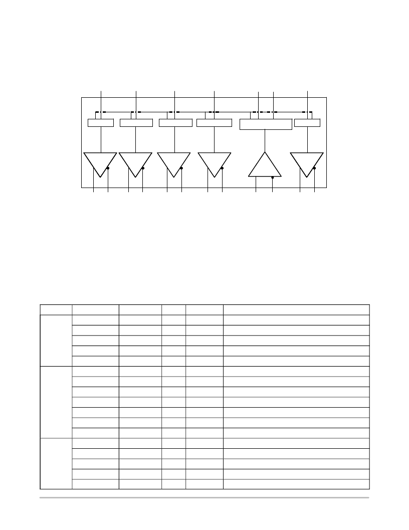
LVDS Block
The LVDS block is positioned below the data block. It
receives a differential clock signal, transmits differential
data over the 12 data channels, and transmits a LVDS clock
signal and a synchronization signal over the clock and
synchronization channel.
A number of LVDS transmitter blocks are placed in
parallel to serve all data, clock, and synchronization output
channels. A high level overview is illustrated in the
following figure.
Serializer
LVDS
Transmitter
clock
Se rialize r<0 >
LVDS
Transmitter
<0>
Serializer <1>
LVDS
Transmitter
<1>
… Serializer <11>
LVDS
Transmitter
<11>
cloc kge nerato r
LVDS
Se rializer
LVDS
Transmitter
Synch
Receiver
Figure 8. LVDS Block ? High Level Overview
The function of this block is to take 10 bits of the protocol
block, serialize these bits, and converts them to an LVDS
standard (TIA/EIA 644A) compatible differential output
signal. The block must also provide a clock to the host, to
allow data recovery. This clock is an on-chip version of the
clock coming from the host.
Sequencer and Logic
The sequencer generates the complete internal timing of
the pixel array and the readout. The timing can be controlled
by the user through the SPI register settings. The sequencer
operates on the same clock as the data block. This is a
division by 10 of the input clock (internally divided).
Table 9 lists the internal registers. These registers are
discussed in detail in Detailed Description of Internal
Registers on page 15.
Table 9. INTERNAL REGISTERS
Block
MBS
(reserved)
LVDS clk
divider
Register Name
Fix1
Fix2
Fix3
Fix4
Fix5
lvdsmain
lvdspwd1
lvdspwd2
Address [6..0]
0
1
2
3
4
5
6
7
Field
[7:0]
[7:0]
[7:0]
[7:0]
[7:0]
[3:0]
[7:4]
[7:0]
[5:0]
Reset Value
0x00
0xFF
0x00
0x00
0x08
‘0110’
0
0x00
0
Description
Reserved, fixed value
Reserved, fixed value
Reserved, fixed value
Reserved, fixed value
Reserved, fixed value
lvds trim
clkadc phase
Power down channel 7:0
Power down channel 13:8
[6]
[7]
0
0
Power down all channels
lvds test mode
Fix6
8
[7:0]
0x00
Reserved, fixed value
AFE
afebias
afemode
9
10
[3:0]
[2:0]
‘1000’
‘111’
afe current biasing
vrefp, vrefm settings
[5:3]
[6]
‘000’
0
Pga settings
Power down AFE
afepwd1
11
[7:0]
0x00
Power down adc_channel_2x 7 to 0
http://onsemi.com
11
发布紧急采购,3分钟左右您将得到回复。
相关PDF资料
NOIV1SE025KA-GDC
IC IMAGE SENSOR 25MP 355PGA
NP100P04PDG-E1-AY
MOSFET P-CH -40V MP-25ZP/TO-263
NP100P04PLG-E1-AY
MOSFET P-CH -40V MP-25ZP/TO-263
NP100P06PDG-E1-AY
MOSFET P-CH -60V MP-25ZP/TO-263
NP100P06PLG-E1-AY
MOSFET P-CH -60V MP-25ZP/TO-263
NP109N04PUJ-E1B-AY
MOSFET N-CH 40V MP-25ZP/TO-263
NP109N055PUJ-E1B-AY
MOSFET N-CH 55V MP-25ZP/TO-263
NP110N03PUG-E1-AY
MOSFET N-CH 30V MP-25ZP/TO-263
相关代理商/技术参数
NOIL2SM1300A-GDC
功能描述:IC IMAGE SENSOR LUPA1300 168PGA RoHS:是 类别:传感器,转换器 >> 图像,相机 系列:* 标准包装:480 系列:- 象素大小:6.7µm x 6.7µm 有源象素阵列:768H x 488V 每秒帧数:52 电源电压:3.3V 类型:CMOS 成像 封装/外壳:48-QFP 供应商设备封装:48-QFP 包装:托盘 请注意:* 配用:4H2105-ND - HEADBOARD FOR KAC-004014H2104-ND - KIT EVAL FOR KAC-00401 其它名称:4H20954H2095-NDKAC-00401-CBC-LB-A0
NOIL2SM1300A-GWC
功能描述:IC IMAGE SENSOR LUPA1300 168PGA RoHS:是 类别:传感器,转换器 >> 图像,相机 系列:* 标准包装:480 系列:- 象素大小:6.7µm x 6.7µm 有源象素阵列:768H x 488V 每秒帧数:52 电源电压:3.3V 类型:CMOS 成像 封装/外壳:48-QFP 供应商设备封装:48-QFP 包装:托盘 请注意:* 配用:4H2105-ND - HEADBOARD FOR KAC-004014H2104-ND - KIT EVAL FOR KAC-00401 其它名称:4H20954H2095-NDKAC-00401-CBC-LB-A0
NOIS1SC1000A-HHC
制造商:ON Semiconductor 功能描述:STAR1000 COLOR JLCC84 - Trays 制造商:ON Semiconductor 功能描述:IC IMAGE SENSOR STAR1000 84JLCC
NOIS1SM0250A-HHC
制造商:ON Semiconductor 功能描述:STAR250 JLCC84 - Trays 制造商:ON Semiconductor 功能描述:IC IMAGE SENSOR STAR250 84JLCC
NOIS1SM0250A-WWC
制造商:ON Semiconductor 功能描述:STAR250 WAFER SALES - Waffle Pack
NOIS1SM0250S-HHC
制造商:ON Semiconductor 功能描述:STAR250 JLCC84 SPACE - Trays 制造商:ON Semiconductor 功能描述:IC IMAGE SENSOR STAR250 84JLCC
NOIS1SM1000A-HHC
制造商:ON Semiconductor 功能描述:Image Sensor Monochrome CMOS 1024x1024Pixels 84-Pin JLCC Tray 制造商:ON Semiconductor 功能描述:STAR1000 JLCC84 - Trays 制造商:ON Semiconductor 功能描述:IC IMAGE SENSOR STAR1000 84JLCC
NOIS1SM1000S-HHC
制造商:ON Semiconductor 功能描述:Image Sensor Monochrome CMOS 1024x1024Pixels 84-Pin JLCC Tray 制造商:ON Semiconductor 功能描述:STAR1000 JLCC84 SPACE - Trays 制造商:ON Semiconductor 功能描述:IC IMAGE SENSOR STAR1000 84JLCC
